Research & Development
WACKER’s research and development activities pursue three goals:
- We contribute to our customers’ market success by searching for solutions that meet their needs.
- We optimize our processes in order to be the technology leader and to be sustainably profitable.
- We concentrate on creating innovative products and applications for new markets and on serving future trends, such as the increase in mobility, urbanization and digitalization, and the rise in prosperity.
R&D Expenses
| Download XLS |
|
|
|
||||||||
€ million |
2016 |
2015 |
2014 |
2013 |
2012 |
|||||
|
|
|
|
|
|
|||||
|
|
|
|
|
|
|||||
Research and development expenses |
183.4 |
175.3 |
183.1 |
173.8 |
173.7 |
|||||
|
|
|
|
|
|
|||||
The R&D rate – research and development spending as a percentage of Group sales – was 3.4 percent (2015: 3.3 percent). It was at the prior-year level despite the positive sales trend, since our expenses climbed in areas such as process engineering.
In 2016, we received about €3.0 million from licensing agreements (2015: €4.2 million). We filed 116 patent applications in 2016 (2015: 114). Our portfolio contains about 5,600 active patents worldwide, as well as 1,900 patent applications currently pending. We license very little R&D know-how from third parties. When we collaborate with universities on research, the results are usually made available to us free of charge or by transfer of rights of use.
New-Product Rate (NPR)1
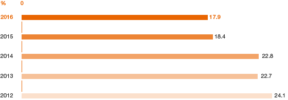
1 Percentage of sales accounted for by products launched in the last five years
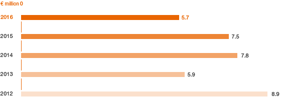
Among our investments were new pilot reactors, in which the production of successful product developments is scaled up from laboratory quantities to industrial volumes. One example is the pilot reactor at WACKER POLYMERS in Nanjing, China. Additional investments included upgrades to laboratory facilities at our subsidiaries in China, South Korea and India in order to facilitate R&D carried out locally at customer locations.
Investments in R&D Facilities
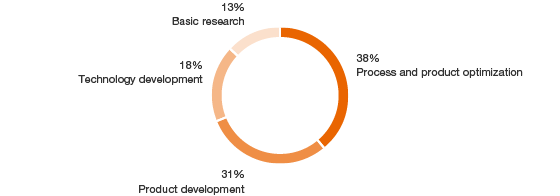
The development of new products and production processes accounted for the majority of our R&D costs. WACKER scientists are currently working on some 300 projects based on more than 30 technology platforms. WACKER operates in highly promising fields, ranging from energy recovery and storage, electronics, automotive engineering and construction to household, medical, health-care and cosmetics products to food and biotechnology.
In 2013, we launched the New Solutions initiative, the goal of which is to rapidly develop technically and commercially superior solutions for new applications. Expertise from all over the company is consolidated groupwide and applied to projects as needed. We have conducted market launches of new and existing products for innovative applications under this initiative, one of these being 3D printing.
Some of our research projects are subsidized by government grants. They include the OPERA (Organic Phosphor for Efficient Remote LED Applications) project, which we completed in 2016. The objective of this EU-sponsored project was to develop LED-based optical components that could enhance luminous efficacy by means of remote phosphor technology (separation of the LED chip from the phosphor layer that generates the white light) and, for example, function as a substitute for daylight. Between 2013 and 2016, six project partners from Germany, Finland and the Netherlands developed novel optical components for the scattering, reflection and transmission of light.
Breakdown of R&D Expenditures
Research and Development at Two Levels
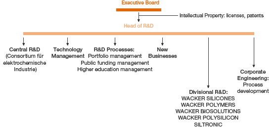
WACKER conducts R&D at two levels: centrally at our Corporate Research & Development department and locally at our business divisions. Corporate R&D coordinates activities on a company-wide basis and involves other departments, such as Corporate Engineering (during process development). We also use a management process to keep our R&D projects transparent throughout the Group. We manage our product and process innovations groupwide in Project System Innovation (PSI), our project management system, where we systematically evaluate customer benefit, sales potential, profitability and technology position.
R&D Organization
Strategic Collaboration with Customers and Research Institutes
Our business divisions conduct application-driven R&D. They focus on product and process innovations in semiconductor technology, silicone and polymer chemistry, and biotechnology, as well as on new processes for producing polycrystalline silicon. We collaborate with customers, scientific institutions and universities to achieve successful research results more quickly and efficiently. In 2016, WACKER worked together with more than 40 international research institutes from three continents on some 44 research projects. Our collaborative efforts cover topics that include electricity storage, process simulation and process development.
WACKER attaches considerable importance to fostering young scientific talent and maintaining close contacts with universities. In 2016, we sponsored some 170 degree theses and internships with students at over 60 universities worldwide. In 2006, Wacker Chemie AG joined with the Technical University of Munich (TUM) to establish the Institute of Silicon Chemistry, located on TUM’s Garching research campus near Munich, and has funded the institute since then.
Since 1987, we have honored outstanding research with the WACKER Silicone Award. Dr. Alexander Filippou, Professor of Inorganic Chemistry at the University of Bonn, Germany, was our award recipient in 2016. We presented what is now the 16th edition of the award to Dr. Filippou at the eighth European Silicon Days in Poznań, Poland.
Research Work at WACKER
As the center of WACKER’s R&D activities, Corporate R&D has the task of researching scientific correlations to develop new products and processes efficiently. Another task is to harness and develop new business fields that complement the Group’s core competencies. Our scientists and engineers conduct basic research, develop new products and processes, and improve existing processes. The lab and technical staff at our R&D, applications-technology and production-support facilities work in our laboratories and in our production and pilot plants, and also support application trials on-site at our customers.
Employees in R&D as of December 31
| Download XLS |
|
|
|
||||||||||
Number |
2016 |
2015 |
2014 |
2013 |
2012 |
|||||||
|
|
|
|
|
|
|||||||
|
||||||||||||
|
|
|
|
|
|
|||||||
Group R&D employees |
1,060 |
1,043 |
1,061 |
987 |
1,008 |
|||||||
R&D ratio1, groupwide (%) |
6.2 |
6.1 |
6.4 |
6.2 |
6.2 |
|||||||
R&D employees, Germany |
830 |
821 |
833 |
817 |
849 |
|||||||
R&D employees, international |
230 |
222 |
228 |
170 |
159 |
|||||||
|
|
|
|
|
|
|||||||
Alexander Wacker Innovation Award
The Alexander Wacker Innovation Award, a €10,000 prize bestowed annually since 2006, recognizes excellence in categories alternating between product innovation, process innovation and basic research. In 2016, WACKER honored a team of four researchers in the process innovation category. They had developed our new 3D printing process for manufacturing printed silicone parts. Our 3D printing technology, launched under the ACEO® brand, uses the “drop-on-demand” method, in which the printer head deposits tiny silicone droplets on a substrate. Layer by layer, the droplets become the workpiece, which ultimately does not differ much from injection-molded parts. With the aid of water-soluble support materials, it is possible to make parts with complex geometries, even those with an internal structure. Customer sectors for 3D printing include medical technology, the automotive industry (e. g. for prototypes) and the aerospace industry.
Siltronic Inventor Award
Siltronic AG confers its Inventor Award, also endowed with €10,000, on employees who have produced technological innovation. The 2016 prize went to a team of two Burghausen employees and one from the Freiberg site. They had developed a new pp epitaxial wafer that is harder and exhibits less tension within the crystal lattice. The electronic components manufactured from it deliver better performance.
Selected Corporate R&D Research Topics
We have set a new research focus on the chemistry of low-valence silicon. The Institute of Silicon Chemistry at the Technical University of Munich is working on this topic, with the aim of implementing the findings in industrial applications such as catalysis in the medium to long term. Our research and development work on silicon-containing anode-active materials for lithium-ion batteries have advanced to a stage where we now fulfill the market requirements for capacity and stability of charge-discharge cycles in the next generation of batteries. We submit our materials to global technology leaders for testing.
In our silicone copolymer technology platform, we are focused on manufacturing processes and additives for plastics. Here, we are improving the properties of casting resins and optimizing processes for the extrusion of plastics, employing renewable raw materials such as wood as fillers, in particular.
Selected Divisional Research Projects
New materials for electrical insulation and heat management to improve conductivity in electronics applications are at the focus of our research teams at WACKER SILICONES. The division is also working on electroactive silicone polymers (EAP s) for sensors and actuators. Silicones featuring enhanced adhesive strength and gentle removal offer better wound care and targeted delivery of actives. In consumer care, we are developing silicone particles with new functionalities for cosmetics applications and to achieve better hold in hair-care products.
WACKER POLYMERS focuses its research on polymers that allow the formulation of low-emission end products, thereby fulfilling the requirements of the most stringent ecolabels. We are working hard to make products that are free of alkylphenol ethoxylate (APEO) surfactants and formaldehyde, and low in volatile organic compounds (VOC s). Examples include functionalized polymer dispersions for cementitious sealing compounds and interior dispersion paints, as well as polymer dispersions for use as finishes for mineral-based surfaces.
WACKER BIOSOLUTIONS has successfully implemented its ESETEC® 2.0 process in manufacturing an antibody fragment for MedImmune, the global biologics research and development arm of AstraZeneca. Our technology has been found to deliver improved productivity and simplified purification processes. The division’s new CANDY2GUM® technology enables the addition of water-based, fat-containing and natural ingredients such as fruit juice, cocoa and coffee in a boiling process to produce chewy candy that turns into chewing gum during consumption. We have also developed a 3D printing process for customizable chewing gum shapes.
WACKER POLYSILICON’s newly commissioned production site in Tennessee, USA, is equipped with an energy-efficient generation of deposition reactors delivering higher output. Technological progress in the development of solar modules is proceeding by leaps and bounds. Our customers have steadily reduced both cutting waste and wafer thicknesses. Cell efficiency is being elevated in parallel. The highest cell efficiencies can be achieved only with hyperpure polycrystalline silicon of the kind produced by WACKER POLYSILICON. Cell efficiency is over 18 percent for multicrystalline standard cells and around 20 percent for monocrystalline cells. High-efficiency monocrystalline cells have efficiency levels ranging from over 20 to as much as 25 percent. At the same time, our customers are continuously enhancing the efficiency of their modules, with commercial solar modules performing at efficiencies as high as 22 percent. The energy payback time, which is the service life of a photovoltaic module required to generate the energy expended for its manufacture, varies by geographical location from six months (in the Sahara) to 18 months (in northern Europe).
Our Siltronic division supports its customers with multi-year design-rule projects aimed at achieving steady integration-density increases on memory chips and microprocessors. The quality parameters of the wafers we produce are flatness and absence of ever smaller surface defects. We are thus contributing to making the sensors installed in cameras and other small electronic devices more compact. In addition, we are providing the basis for higher performance in power electronics by improving the efficiency of components such as power supply units. With its custom-designed development projects, Siltronic serves many specialty applications such as electromobility and Industry 4.0.
Key Product Launches in 2016
|
|||
Product |
Description |
Application |
Sector |
|
|
|
|
ACEO® Imagine Series K |
Industrial-scale 3D printer for silicone rubber |
Additive manufacturing of prototypes, small series and assemblies with complex geometries |
Prototyping, aerospace, medical and biomodeling |
BELSIL® REG 1102 |
Film-forming silicone resin elastomer gel |
Skincare lotions and sunscreens, make-up |
Cosmetics |
ELASTOSIL® LR 3003 / 90 |
Silicone elastomer with high Shore hardness |
Large-scale production of dimensionally stable silicone products and hard / soft composites |
Plastics |
ELASTOSIL® LR 5040 |
Liquid silicone rubber with substantially reduced VOC content |
Babycare, medical technology, food processing |
Plastics |
GENIOPLAST® for Wood-Plastic Composites |
Thermoplastic silicone additives |
Manufacture of wood-polymer composites |
Wood processing |
LUMISIL® 590 & 591 |
High-refractive-index silicone |
High-performance LEDs, optical components |
Manufacture of LEDs |
LUMISIL® LR 7601 |
Highly transparent liquid silicone rubber with substantially reduced VOC content |
Optical lenses, sensors and coupling elements in lighting technology |
Plastics |
SILPURAN® 2122 |
Gelatinous silicone adhesive |
Adhesive plasters, therapeutic tapes |
Wound care |
VINNAPAS® EP 3360 ULS |
VAE dispersion |
Environmentally compatible interior paints |
Paints and coatings |
CAVAMAX® W6 |
Alphadextrin |
Vegetarian-grade emulsifier-substitute for baked goods |
Food |
WACKER process to produce Spectrila® |
Microbial manufacturing process for biologics |
Cost-efficient production of a leukemia medication for children |
Pharmaceuticals |
VINNAPAS® 5005 N |
VAE dispersible polymer powder |
Cost-efficient binder for dry-mix mortars |
Construction |
