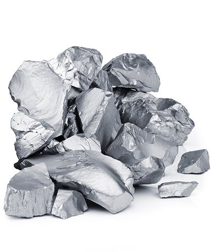
Polysilicon
Purity Is Our Recipe for Success
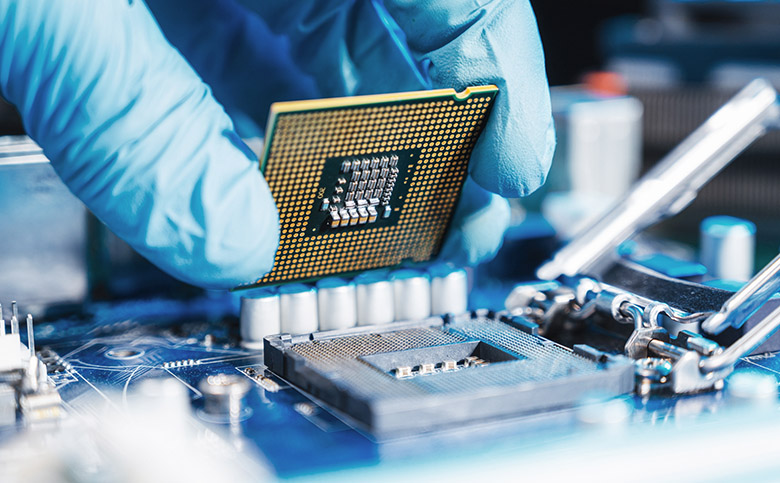
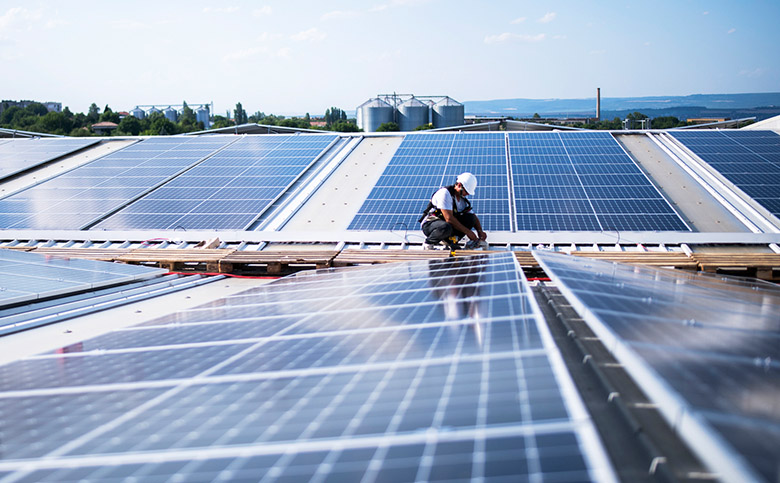
Polysilicon is indispensable for high-performance semiconductors and solar cells. WACKER is the only European company to rank among the global market leaders in this highly competitive business – a position primarily due to the exceptionally high quality that WACKER offers its customers. With its highly efficient production processes and uncompromising quality standards, the company has succeeded in maintaining and further expanding its position despite the high energy prices in Europe.
The plant is unusually quiet for a production environment. The reactors, which stand in long rows in a hall about the size of ten tennis courts, emit only a low hum. A plant operator takes a quick look through the small, round sight glasses to inspect the interior of the enormous metal domes, which give off an orange glow. Otherwise, the production hall is deserted.
We are standing in the deposition hall, the heart of polysilicon production in Burghausen. The reaction taking place here is known as the “Siemens process,” which involves feeding trichlorosilane into reactors at a temperature of about 1,000 degrees Celsius, at which point high-purity polysilicon deposits onto seed rods. After several days, when the rods have grown to the desired diameter, the reactors are shut down and opened, and the polysilicon rods are removed and broken into smaller pieces. These then undergo an additional, complex cleaning process for semiconductor applications. Finished and packaged, the polysilicon pieces go to the customers – manufacturers of semiconductor and solar wafers all over the world.
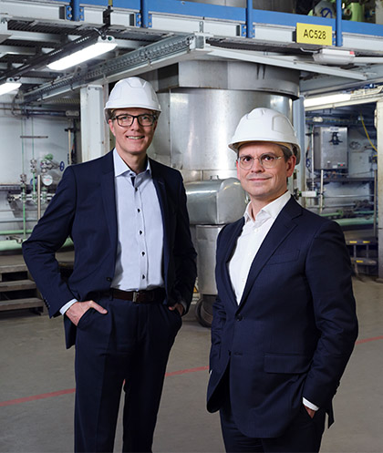
What sounds so simple is actually a very complex process that requires sophisticated technology and, above all, decades of experience. “The production facilities we see here are almost entirely in-house developments,” says Tobias Brandis, not without pride. “What’s more, WACKER’s been producing polysilicon since the late 1950s, first in Burghausen, then in Nünchritz starting in 2011 and, as of 2016, in Charleston.”
“When it comes to electronic-grade silicon, WACKER is by far the world market leader.”
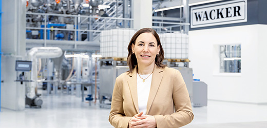
According to Brandis, who has a doctorate in law and has served as president of the WACKER POLYSILICON division since 2017, WACKER is now one of the global market leaders in this business. This is particularly true of polysilicon for semiconductors, which has to be much purer than the material for solar cells. “WACKER is by far the market leader in this area and the only supplier to offer products for all production processes – from polysilicon pieces in various sizes for crucible pulling to polysilicon rods for float-zone pulling. Almost every other microchip in the world is made with our polysilicon, whether it’s in a supercomputer, a smartphone or a car,” Brandis explains.
When asked about the recipe for success that has enabled WACKER to achieve this market position, Brandis has a clear answer: “Quality, quality and more quality.” Everything revolves around the purity of the polysilicon – the indispensable prerequisite for ever more powerful microchips. Producing the starting material gets things going. Metallurgical silicon is converted to liquid trichlorosilane using hydrogen chloride and then purified in tall distillation columns. Other substances that are still contained in the silicon metal, such as iron, copper, nickel, boron and phosphorus, are almost completely removed in the process. The reason? Increasing the purity of the polysilicon allows manufacturers to make smaller and faster microchips. “We’re talking about concentrations of critical impurities in the parts-per-trillion range,” Brandis explains. One ppt corresponds to a concentration of 10 grams of sugar in ten billion liters of water – the volume of one million tank trucks.
Manufacturing electronic-grade silicon is an art mastered by very few other producers besides WACKER. But that alone is not enough to achieve market success, Brandis warns: “The second lever is cost.” Having its production in Germany puts WACKER at a clear disadvantage relative to competitors in other regions. After all, production of polysilicon is extremely energy intensive. “Electricity is by far our single biggest cost item in manufacturing,” Brandis observes, cutting to the chase. In China, home to most of WACKER’s competitors on the solar polysilicon market, electricity prices were four to five times lower than in Europe, he said. But electricity is also significantly cheaper in the US and other Asian countries than it is in Germany.
One of WACKER’s answers to this challenge lies in integrated production, a system that involves either feeding byproducts and wastes back into the production cycle or processing them to make other products. Sophisticated energy management likewise reduces power consumption. The waste heat generated by cooling the polysilicon, for example, generates steam for distillation. Over the decades, WACKER has continuously optimized the energy efficiency of its polysilicon production. “Today, we need only half as much energy to produce one kilogram of polysilicon as we did 20 years ago,” Brandis notes.
Uncompromising quality and energy efficiency in production – that’s the formula WACKER has used in recent years to steadily expand its market position in polysilicon for semiconductors and ultrahigh-efficiency solar cells. “We’ve doubled our volumes of semiconductor polysilicon since 2017 and reduced our total costs by a quarter in the process,” says Brandis, setting the tone for the future. His business division is aiming for yet another major increase in semiconductor material production volumes by 2030. At the same time, the company also intends to enhance quality still further in order to support the semiconductor industry as it continues to develop. The goal is to generate an EBITDA margin of more than 30 percent by the end of this decade and to earn twice the cost of capital. To accompany this planned growth, WACKER POLYSILICON is significantly increasing its investments, with some 100 million euros per annum going toward expansion projects over the next few years. The focus here is on capacities and on initiatives addressing the quality of the semiconductor material.
“Demand for semiconductor wafers will again increase significantly in the coming years.”
As Wolfgang Storm knows, the prospects for this growth are very good. Storm is an old hand when it comes to the polysilicon business. A Ph.D. physicist, he joined Chemitronic, the predecessor of today’s Siltronic AG, back in 1996 and has worked in strategic marketing at WACKER POLYSILICON since 2009. Having analyzed the semiconductor and solar markets for decades, Storm has seen many ups and downs in the industry.
“I have no doubt that demand for semiconductor wafers will again increase significantly in the coming years,” he says with conviction. He estimates that semiconductor wafers with a surface area of around 115 billion square centimeters were sold worldwide last year – about as much as 1,600 soccer fields. That figure is expected to grow to about 170 billion square centimeters by 2030, or about 50 percent more than today. “That growth won’t be linear, of course: we’ll see fluctuations just as we have in the past, but the trend is clear,” Storm believes. Driving that trend is the unrelenting advance of digitalization and the new applications it brings to every aspect of our lives. And more wafers automatically mean correspondingly greater demand for polysilicon of the highest quality.
WACKER is benefiting from the fact that the semiconductor industry’s demands on its polysilicon suppliers are constantly increasing. The structures of microchips, the design rules, are becoming smaller and smaller in order to accommodate even more transistors on them and thus make them even more powerful. “We’re now talking about a design rule of two nanometers for 300-millimeter wafers – one 25-thousandth of a human hair,” Storm explains, adding that the only way to do that is with polysilicon which has virtually no impurities left. The requirements are similarly high for the production of CMOS image sensors, i.e. the light-sensitive chips in smartphone cameras, or for filters for 5G/6G mobile communications – indispensable components of self-driving vehicles.
In the short term, he believes it is unlikely that the expected growth of the semiconductor industry would prompt new competitors to begin producing polysilicon for demanding applications like these: “Basically, very few companies other than WACKER can make that kind of ultrapure polysilicon in any relevant quantities. And in the semiconductor industry, the process of qualifying a new supplier for material like that takes years.” Ideal conditions, in other words, for WACKER to remain on the road to success in the semiconductor business in the years ahead, thanks to its technological edge.
Float-Zone Pulling for Power Electronics
Power semiconductors play an important role not only in the field of electrical infrastructure, but also for electromobility. Of particular interest here are “insulated gate bipolar transistors” (IGBTs), which are mainly found in hybrid and electric vehicles, in wind turbines and solar installations, as well as in smart grids. Unlike the Czochralski process, float-zone pulling does not involve drawing the monocrystal from a crucible. Instead, a polysilicon rod is melted with an induction coil, and, when in contact with a seed crystal, the original polycrystalline rod yields a monocrystal. This method allows manufacturers to produce wafers with very high, uniform electrical resistance values combined with the low oxygen content required for power electronics. WACKER is one of very few polysilicon manufacturers in the world to offer special polysilicon rods for the float-zone method. Up to 230 centimeters long, these rods are polished with exceptional precision to a diameter specified by the customer, and when appropriately surface-treated, can be used immediately in wafer production without any additional prep work.
WACKER POLYSILICON – Strategy and Goals
Gaining a Lead through Very High Quality
Growth
Twofold increase (volumes of electronic-grade silicon (EGS))
Profitability
EBITDA margin > 30 percent ROCE > 2x cost of capital
Specific investment focus
Expansion of EGS capacity
Focus markets
Semiconductor wafers, solar cells with extremely high efficiencies
WACKER is the clear No. 1 in polysilicon for the semiconductor sector. Nearly half of the computer chips produced worldwide use the division’s hyperpure polysilicon. WACKER POLYSILICON has doubled sales in this high-growth market over the last five years and intends to continue strengthening its position in the semiconductor sector in the next few years. The division is aiming for yet another major increase in semiconductor-material production volumes by 2030. At the same time, the company also intends to enhance quality still further in order to support the semiconductor industry as it continues to develop. Absolute quality is likewise essential for the material that WACKER POLYSILICON supplies for solar applications. In this field, the division is one of the few suppliers capable of offering particularly high-quality polysilicon for monocrystalline solar cells with extremely high efficiencies. Another aim is to make production processes even more efficient so as to further reduce production costs. WACKER POLYSILICON intends to generate an EBITDA margin of more than 30 percent in 2030 and earn more than twice its cost of capital. To achieve this planned growth, WACKER POLYSILICON is significantly increasing its capital expenditures, with some 100 million euros per annum going toward expansion projects over the next few years. The focus here is on expanding EGS capacity. Long-term customer contracts will secure these investments.