Research & Development
WACKER’s research and development pursues three goals.
- Firstly, we contribute to the market success of our customers by searching for solutions that meet their needs.
- Secondly, we optimize our processes in order to be the technology leader and to be sustainably profitable.
- Thirdly, we concentrate on creating innovative products and applications for new markets and on serving future trends, such as higher energy requirements, urbanization, digitalization and growing prosperity.
R&D Expenses
| Download XLS |
|
|
|
||||||||||||
€ million |
2015 |
2014 |
2013 |
2012 |
2011 |
2010 |
2009 |
|||||||
|
|
|
|
|
|
|
|
|||||||
Research and development expenses |
175.3 |
183.1 |
173.8 |
173.7 |
172.9 |
165.1 |
164.0 |
|||||||
|
|
|
|
|
|
|
|
|||||||
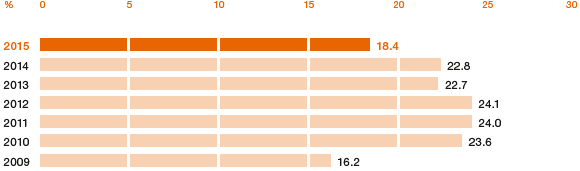
R&D expenditures in 2015 amounted to € 175.3 million (2014: € 183.1 million). At 3.3 percent (2014: 3.8 percent), the R&D rate – research and development spending as a percentage of Group sales – was down from the prior-year figure due to the positive sales trend and lower expenses.
New-Product Rate (NPR)1

1 Percentage of sales accounted for by products launched in the last five years
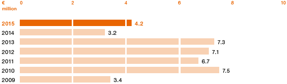
We received about € 4.2 million from licensing agreements in 2015 (2014: € 3.2 million). WACKER’s innovative strength is reflected in the number of patents held and patent applications submitted. In 2015, we filed 114 patent applications (2014: 111). Our portfolio contains about 5,300 active patents worldwide, as well as 2,000 patent applications currently pending.
Licensing Income

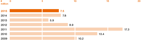
In 2015, WACKER invested € 7.5 million in R&D facilities (2014: € 7.8 million). Among our investments were new pilot reactors, where positive project results are scaled up and then converted to full production. Examples include polymerization reactors at WACKER POLYMERS and deposition reactors at WACKER POLYSILICON. Additional investments included equipping laboratories to facilitate R&D carried out locally at customer locations. We have invested in analytical equipment that will provide us with quick and precise results for use in the evaluation of experiments.
Investment in R&D Facilities

Breakdown of R&D Expenditures
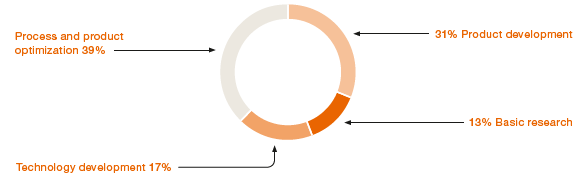

Most of the € 175.3 million (2014: € 183.1 million) in R&D costs was spent on the development of new products and production processes. WACKER scientists are currently working on some 260 projects based on more than 40 technology platforms. 24 percent of these topics are key strategic projects that account for 36 percent of all project costs (totaling € 67.3 million) incurred in 2015. WACKER operates in highly promising fields, ranging from energy, electronics, construction and automotive engineering to household and personal-care products, food and biotechnology.
In 2013, we launched the New Solutions initiative, the goal of which is to develop technically and commercially superior solutions for new applications. Expertise from various parts of the company is consolidated groupwide and applied to projects as needed. In 2015, we started a new project under this initiative. The market and technology evaluations of this project reveal potential additional sales worth hundreds of millions of euros. The first product developments from this initiative are currently in the market launch phase.
In 2015, we spent some € 208,000 (2014: € 768,000) on third-party R&D expertise acquired from four different partners.
Some of the research projects we completed in 2015 were subsidized by government grants. Here are some examples:
- The Federal Ministry of Education and Research (BMBF) subsidizes research related to the energy transition. This includes the iC4 project (Integrated Carbon Capture, Conversion and Cycling), which received € 6.3 million in funding between 2012 and 2015. The goal is to use surplus green electricity for water electrolysis. The resulting hydrogen is converted to methane gas with the aid of carbon dioxide and then stored in the gas grid. WACKER, Clariant, E.ON, Linde, MAN and Siemens were involved in the project, as are eight institutes at the Technical University of Munich and the Fraunhofer Institute for Interfacial Engineering and Biotechnology. WACKER headed two of the four subprojects.
- The goal of the SafeBatt project was to develop battery components that would increase the safety and reliability of lithium-ion batteries (LIBs) for electric vehicles. Between 2012 and 2015, 14 project partners from industry and the scientific community developed materials, models, test methods, sensors and evaluation electronics. The Federal Ministry of Education and Research (BMBF) provided funding for SafeBatt in the amount of € 19 million. WACKER’s work in this group focused on silicon-containing additives for making lithium-ion batteries safer.
- The Alpha-Laion consortium project was started in 2012 to develop high-energy traction batteries for electric vehicles. Bosch headed the project, and the other partners were WACKER, BASF, SGL, BMW and Daimler. In this project, WACKER developed silicon-containing anode materials. Alpha-Laion was funded with € 13 million by the then Federal Ministry of Economics and Technology (BMWi).
During 2015, our business divisions and Central R&D submitted applications for six more projects (in the areas of energy generation and storage, electronics and new materials) to government sponsors, with approvals pending. Our externally-funded research projects are coordinated by our Public Funding office, which evaluates prospective programs, submits our project proposals and manages contacts with funders.
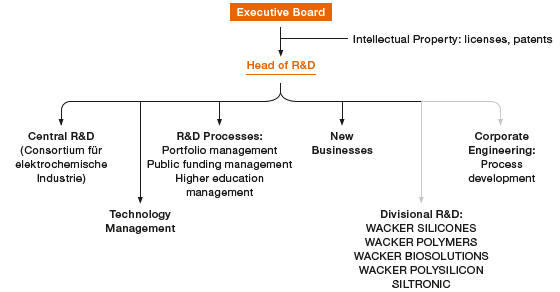
Research and Development at Two Levels
WACKER conducts R&D at two levels: centrally at our Corporate Research & Development department and locally at our business divisions. Corporate R&D coordinates activities on a company-wide basis and involves other departments, such as Corporate Engineering (during process development). We also use a management process to keep our R&D projects transparent throughout the Group. In 2015, we introduced Project System Innovation (PSI), our project management system, to additional subsidiaries.
Strategic Collaboration with Customers and Research Institutes
Our business divisions conduct application-driven R&D. They focus on product and process innovations in semiconductor technology, silicone and polymer chemistry, and biotechnology, as well as on new processes for producing polycrystalline silicon. To achieve successful research results more quickly and efficiently, we collaborate with customers, scientific institutions and universities. In 2015, WACKER worked together with more than 40 international research institutes from three continents on some 50 research projects. Our collaborative efforts cover topics that include electricity storage, biotechnology, process simulation and process development. We have participated in electricity storage projects with universities in Braunschweig, Munich and Münster.
WACKER has also created a worldwide network of 21 technical competence centers, which liaise between sales offices and local production sites. Specialists in these centers customize products to regional requirements, including climatic conditions, national standards and local raw materials. They develop formulations for customers’ new products and also optimize existing recipes.
Research Work at WACKER
As the center of WACKER’s R&D activities, Corporate R&D has the task of researching scientific correlations to develop new products and processes efficiently. Another task is to harness and develop new business fields that complement the Group’s core competencies.
R&D Organization

WACKER had 1,043 research and development staff in 2015, which represents 6.1 percent of the Group’s employees. Our scientists and engineers conduct basic research, develop new products and processes, and improve existing processes. The lab and technical staff at our R&D, applications-technology and production-support facilities work in our laboratories and in our production and pilot plants, or on-site at our customers’ plants. Examples of what our other R&D personnel do include building research equipment in our workshops and performing administrative functions in such fields as market research and trend analysis.
Employees in R&D as of December 31, 2015
| Download XLS |
|
|
|
||||||||||||||||
Number |
2015 |
2014 |
2013 |
2012 |
2011 |
2010 |
2009 |
|||||||||||
|
|
|
|
|
|
|
|
|||||||||||
|
||||||||||||||||||
Group R&D employees |
1,043 |
1,061 |
987 |
1,008 |
1,100 |
1,057 |
1,072 |
|||||||||||
R&D ratio1, groupwide |
6.1 |
6.4 |
6.2 |
6.2 |
6.4 |
6.5 |
6.9 |
|||||||||||
R&D employees, Germany |
821 |
833 |
817 |
849 |
868 |
855 |
860 |
|||||||||||
R&D employees, international |
222 |
228 |
170 |
159 |
232 |
202 |
212 |
|||||||||||
|
|
|
|
|
|
|
|
|||||||||||
R&D employees, Germany, by qualification |
821 |
833 |
817 |
849 |
868 |
855 |
860 |
|||||||||||
Scientists and engineers |
307 |
322 |
318 |
339 |
346 |
337 |
332 |
|||||||||||
Lab staff and technicians |
406 |
341 |
329 |
332 |
350 |
344 |
349 |
|||||||||||
Other personnel |
108 |
170 |
170 |
178 |
172 |
174 |
179 |
|||||||||||
|
|
|
|
|
|
|
|
|||||||||||
R&D employees, international, by qualification2 |
121 |
114 |
102 |
92 |
93 |
95 |
90 |
|||||||||||
Scientists and engineers |
51 |
45 |
38 |
32 |
35 |
31 |
30 |
|||||||||||
Lab staff and technicians |
35 |
37 |
34 |
32 |
30 |
32 |
29 |
|||||||||||
Other personnel |
35 |
32 |
30 |
28 |
28 |
32 |
31 |
|||||||||||
R&D employees, international, Siltronic AG only (without differentiation by qualification) |
101 |
114 |
68 |
67 |
139 |
101 |
122 |
|||||||||||
|
|
|
|
|
|
|
|
|||||||||||
Alexander Wacker Innovation Award
WACKER presented the 2015 Alexander Wacker Innovation Award in the product innovation category to a Burghausen-based researcher who had developed a process for producing ultrathin silicone films. As thin as 10 micrometers, these precision films with their dielectric properties provide the basis for innovative products in such areas as electronics, robotics, sensors and medical technology. Named after the company’s founder, the € 10,000 award has been presented annually since 2006 – alternating between the categories of product innovation, process innovation and basic research.
Siltronic Inventor Award
Siltronic AG confers its Inventor Award, also endowed with € 10,000, on employees who have produced technological innovation. The 2015 prize was awarded for simulation tests that promote higher yields and improve defect monitoring during the silicon-crystal pulling process. Siltronic’s Crystal Growth Control project helped to significantly increase the amount of pulled crystals conforming to customer specifications for what are known as prime wafers.
Selected Corporate R&D Research Topics
One focus of research was wood-plastic composite materials, or WPCs. Wood plastic composites are composed of up to 75 percent wood fiber, for example sawdust, and a thermoplastic polymer such as polypropylene. WPCs can be molded into the desired form with modern plastic technology processes: extrusion, injection and rotational molding, compacting and thermoforming. GENIOPLAST ® PP is a production aid that can substantially raise productivity, which in turn lowers production costs. Areas of application include floor coverings and automotive interior trims.
With ESETEC® 2.0, we offer an efficient method for producing high yields of antibody fragments for medical therapies. One big step achieved by our research on this system was the development of a selectable element that permits stable fermentation without the usual addition of antibiotics. This patented antibiotic-free process for high-yield production of pharmaceutical proteins also contributes to greater safety and environmental compatibility.
Selected Divisional Research Projects
WACKER SILICONES is currently researching a method for using silicones in 3D printing. Uses include the manufacture of components for the automotive industry, for medical or optical applications and for household-care products. To enhance efficiency in paper production, we are developing foam-control agents that remain effective longer at lower concentrations. Our research has discovered new uses for silicone resins as binders, for example in mineral wool or artificial stone, also for use outdoors. We have developed skin-compatible SILPURAN® silicone gels for advanced wound dressings. One variation of these dressings contains plasma, a substance that kills microbes and multiresistant bacteria, and promotes healing.
WACKER POLYMERS focuses its research on polymers that allow the formulation of low-emission end products, thereby fulfilling the requirements of the most stringent ecolabels. In the spirit of sustainability, we have developed and improved products that are free of alkylphenol ethoxylate (APEO) surfactants and formaldehyde, or low in volatile organic compounds (VOCs). Examples of our development efforts are reactive self-crosslinking dispersible polymer powders for cementitious flooring systems and polymer dispersions for finishing mineral-based surfaces. We have intensified our work on silica-polymer composite materials for emulsion paints and wood coatings.
WACKER BIOSOLUTIONS licensed its ESETEC® 2.0 process for manufacturing antibody fragments to MedImmune, AstraZeneca’s R&D division for biologics. The high productivity and simple purification processes offered by our technology help speed up the process of providing new medications to patients.
To improve the energy balance of solar cells and reduce costs, we are striving to further reduce energy consumption in polysilicon production. WACKER POLYSILICON has continued to optimize the processes in its closed production loop, further reducing energy consumption during deposition and conversion. Technological progress in the development of solar modules continues to proceed by leaps and bounds. Our customers have steadily reduced the thickness of wafers: from 450 µm in 1995 to 250 µm in 2005 and to under 200 µm in 2010, with the standard thickness currently around 180 µm. Cell efficiency has risen in parallel, and is now around 18 percent for multicrystalline standard cells and well over 19 percent for monocrystalline cells. High-efficiency monocrystalline cells have efficiency levels ranging from over 20 to as much as 25 percent. The energy payback time, i.e. the service life of a photovoltaic cell required to generate the energy expended for its manufacture, varies according to geographical location from between six months (in the Sahara) and 18 months (in northern Europe).
The performance of semiconductor devices doubles about every two years. Among the key performance-boosting parameters are the design rules achieved on a silicon wafer, which determine how many transistors per square centimeter fit on a device. The semiconductor industry’s standard design rules in recent years of 22 and 16 nanometers (nm) have already been replaced in some cases by an 11 nm standard. In the years to come, we expect this trend to continue and forecast design rules increasingly approaching 8 nm. Siltronic is currently developing processes to produce 300 mm wafers that can be used for these new design rules. In the reporting period, regular shipments of 11 nm wafers continued to increase and we further refined the technology for 8 nm wafers. We worked on wafers for power and LED applications as well as for high-frequency applications in the area of mobile communications.
Transferring Knowledge Locally
Our WACKER ACADEMY locations serve as forums for industry-specific knowledge transfer between customers, distributors and WACKER experts. The focus is on industry-specific courses, which now cover silicone applications in addition to polymer chemistry, such as for cosmetics and paints. The training centers’ proximity to our development and test laboratories promotes the sharing of ideas and enables participants to conduct practical on-site tests. We work with company research facilities, universities and institutes to ensure our seminars remain state of the art.
WACKER attaches considerable importance to fostering young scientific talent and maintaining close contacts with universities. In 2015, we sponsored some 210 final-degree theses and internships with students at over 50 universities internationally. In addition, Wacker Chemie AG and the Technische Universität München (TUM) extended their existing partnership in silicon research for another six years by signing a corresponding agreement in 2014. WACKER and TUM founded the Institute of Silicon Chemistry in 2006.
Key Product Launches in 2015
|
||||||
Product |
Description |
Application |
Sector |
|||
|
|
|
|
|||
BELSIL® EG 1 |
Silicone elastomer gel |
Improved texture of cosmetic formulations |
Cosmetics |
|||
BELSIL® PF 200 |
Phenyl silicone fluid |
Shine of water-based hair and skin care products |
Cosmetics |
|||
BELSIL® REG 102 |
Silicone elastomer gel |
Improved water resistance of cosmetic formulations |
Cosmetics |
|||
DEHESIVE® SFX |
Solvent-free silicone polymer |
Highly efficient coating compound for label release papers and films |
Paper and label industries |
|||
ELASTOSIL® RT 779 |
Condensation-curing two-part silicone rubber |
Silicone adhesive for engine oil pans |
Automotive |
|||
FOLDTEC® |
E. coli-based refolding technology |
Manufacture of highly pure pharmaceutical proteins |
Pharmaceuticals |
|||
GENIOSIL® XT |
Silane-terminated polymers |
Industrial adhesives, liquid waterproofing systems, and coatings |
Automotive, adhesive and sealant industries |
|||
PRIMIS® AF 1000 |
Dispersion |
Innovative binders for dirt- and weather-resistant exterior paints and plasters |
Construction and paints |
|||
PULPSIL® 968 S |
Silicone surfactant |
Energy-saving dewatering formulations |
Pulp and paper manufacturing |
|||
SILPURAN® 2117 |
Silicone adhesive gel |
Skin-compatible, breathable wound dressings |
Healthcare |
|||
SILRES® WH |
Silicone resin emulsion |
Additive for water-repellent wood-protection coatings |
Construction |
|||
SMARGO® |
Dispersible polymer powder |
Binder for dry-mix mortars |
Construction |
|||
VINNAPAS® 4040 E |
Dispersible polymer powder |
Formulation of flexible sealing slurries |
Construction |
|||
VINNAPAS® 4800 G |
Dispersible polymer powder |
Modification of gypsum drywall products |
Construction |
|||
VINNAPAS® 5518 H |
Dispersible polymer powder |
Binder for water-repellent skim coats |
Construction |
|||
VINNAPAS® EF 104 |
VAE dispersion |
Coating of printed paperboard surfaces |
Paper and packaging |
|||
VINNAPAS® EF 8860 |
VAE dispersion |
Formulation of adhesives for flexible floor coverings |
Adhesives |
|||
VINNAPAS® LL 3031 |
Dispersion |
Binder for environmentally compatible interior and exterior paints, as well as plasters |
Construction and paints |
|||
WETSOFT® NE 500 |
Hydrophilic silicone emulsion |
Makes textiles more comfortable to wear |
Textile industry |
|||
WETSOFT® NE 750 |
Anhydrous silicone formulation |
Makes textiles more comfortable to wear |
Textile industry |
|||